■ Research and development fields
Low-K film and stacked CSP
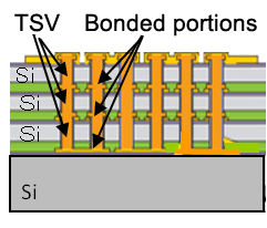
TSV, Cu pillar, fuel cell, etc.
■ Semiconductor packaging
Mold IC, WLP,
MUF, FCBGA
■ Electronic parts and ceramics
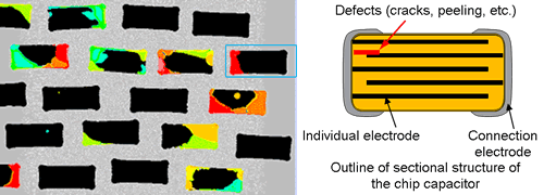
MLCC, chip capacitor
Filter, laminated structure
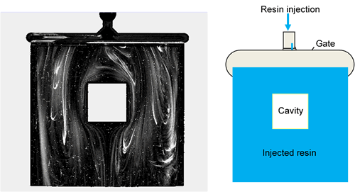
■ Resin / composite materials
Filler observation,
flow observation of injection molding
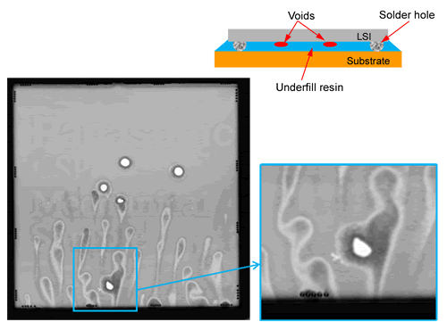
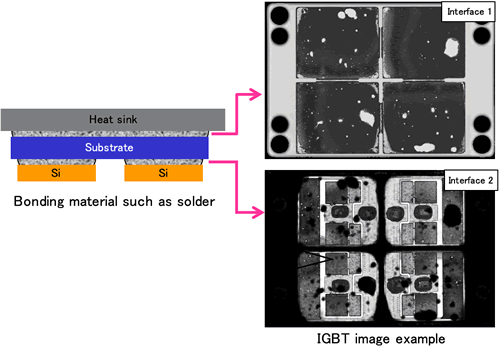
■ Power module
Automotive semiconductor, IGBT,
Cooling system (heat countermeasure)
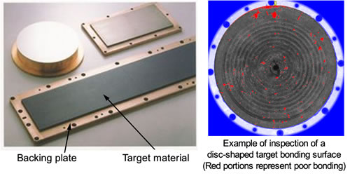
■ Metal products and target materials
Brazed portions, deposited portions
Cracks, voids, deterioration
■ MEMS
Sensors, SOI,
Bonded wafers
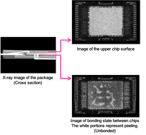
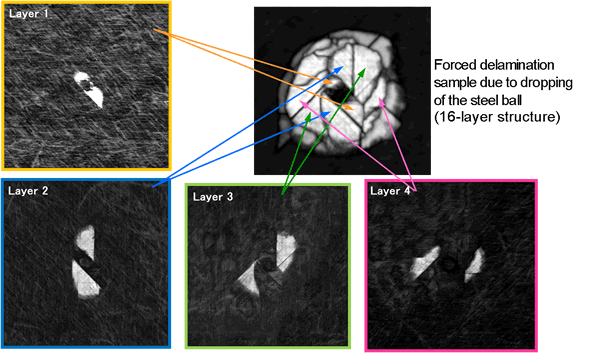
The following show the types of the applications and defects that can be inspected by the ultrasonic imaging apparatus FineSAT.
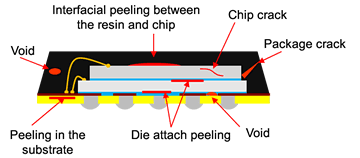
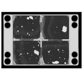
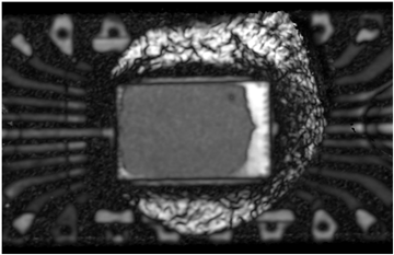
Example of the IC package cross section
The following examples show the detected cracks, peeling and voids between internal electrodes of chip parts.
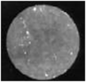
The target material for the sputtering target is used for forming semiconductors, FPDs and electrodes of solar cells, etc. FineSAT is used to inspect the bonding state between the target material and the backing plate.
The apparatus compatible with the enlargement of the target material enables the inspection.
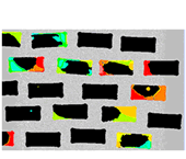
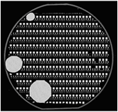
FineSAT is applied to the in-line inspection of bonding portions of various parts including IGBT. Regardless of size, the white spots and areas within the gray frames represent all peeling off and voids.
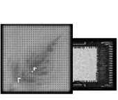
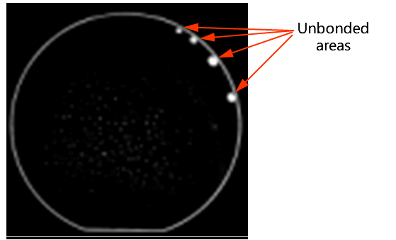
The following example shows the image of the bonded surface of the bonded wafer used for MEMS.
Depending on the conditions, it is also possible to detect the unbonded portions with a diameter of 10 μm.
The electronic scanning system has high throughput that enables the total inspection of mass-produced products and is suitable for the in-line total inspection.
Based on the electronic scanning system-inspection apparatus such as ES5100 series (standard model), we can also manufacture the automatic inspection apparatus by adding an automatic transportation function, an automatic judgment function, etc. according to the customer's product and production line.
We will select the appropriate technology from a wide range of our technologies and customize it, so please do not hesitate to consult us.
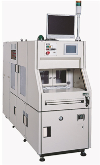
Semi-automatic inspection apparatus
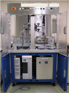
Fully automatic inspection apparatus
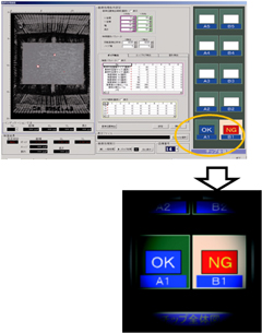
The advanced image processing technology is incorporated into the high-speed display image technology by electronic scanning, and the acceptance or rejection (OK / NG) of the product is judged.
Total inspection before shipment assists in assuring quality.
The figure on the left is an example of judging OK / NG in real time with the automatic GUI monitor.
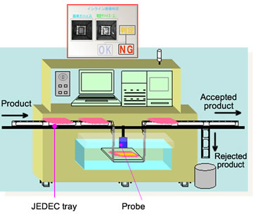
This apparatus also makes it possible to inspect products on JEDEC trays and add a function to remove defective products from the production line after judging non-defective / defective products.
In addition, this apparatus makes it possible to grasp the occurrence tendency of defective products (NG products), the defective rate for each production lot, etc. by collecting and storing the measured data after bar-coding each product, which leads to a powerful tool for improving the yield rate.
Please feel free to contact us about various automation of the apparatus.
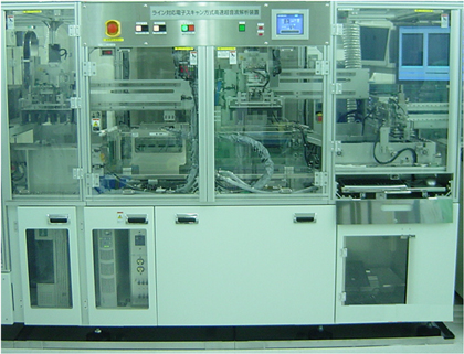
Electronic scanning system-fully automatic inspection apparatus for semiconductor package inspection